Chemical design of functional nanomaterials

At the core of our work lies the development of synthetic strategies—from molecular design to the engineering of complex ink systems—enabling scalable and functional nanomaterial applications. By integrating precision chemical design, structural control, and self-assembly principles, and by innovating in automated and high-throughput synthetic processes, we accelerate discovery and optimization.
Our research is driven by deep expertise in nanomaterial chemistry, where we pioneer innovations across two interconnected yet distinct directions: semiconductor nanocrystals and hard/superhard nanomaterials for extreme environments.
We design and synthesize semiconductor nanocrystals, spanning from conventional to unconventional systems (e.g., perovskites and antiperovskites), with optical and electronic properties tailored from the visible to the infrared. These materials enable breakthroughs in optoelectronics, energy conversion, sensing, and advanced imaging, where we achieve unprecedented control over their synthesis, structure, and surface chemistry.
Simultaneously, we develop hard and superhard nanomaterials, such as metal borides, engineered for extreme environments. These materials combine exceptional mechanical strength, thermal stability, and conductivity, making them ideal for high-temperature electronics, protective coatings, and high-stress applications.
By integrating automated high-throughput synthesis and precision chemical design, we accelerate the discovery and optimization of nanomaterials that are both scientifically innovative and industrially impactful. Our work pushes the boundaries of material science, creating solutions that redefine performance in energy, electronics, and beyond.
Novel semiconductor nanocrystals (part 1)
Novel metal halide/chalcogenide perovskites and antiperovskites show promising properties for incorporation in photovoltaic devices. Lead halide perovskites are extensively studied due to their excellent optoelectronic properties, making them ideal materials for photovoltaic devices. Current setbacks for these materials include the intrinsic toxicity of lead as well as their limited stability in ambient conditions, making the search for stable and highly performant lead-free perovskite materials a difficult necessity.

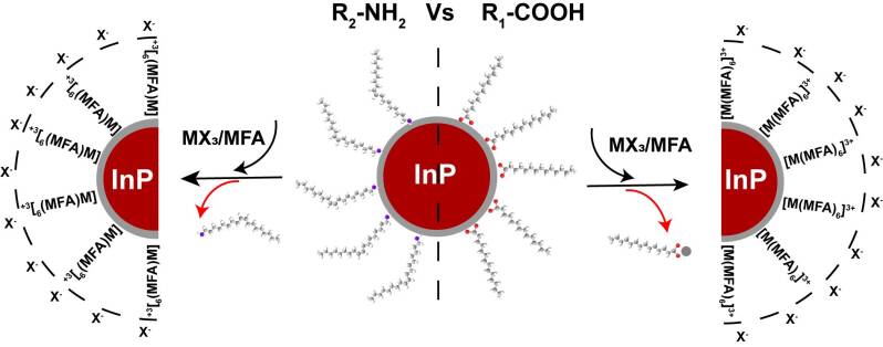
Semiconductor pnictides (such as III-V: GaN, GaAs, InP, InSb, InAs, etc) NCs.
Their chemistry is far behind that of metal NCs or chalcogenides QDs, especially for near and mid-infrared. Therefore, to enhance their performance, we plan to develop new synthetic routes for high-quality and upscalable synthetic methods for core-only and core-shell heterostructure. Their ligands will be optimized for the chemistry of these systems with the aim of obtaining stable inks for the fabrication of high-performance photodetectors. Those QDs-based inks are still a strong candidate as non-toxic active materials, especially for infrared sensing devices that will impact autonomous cars and medicine.
Hard nanomaterials (part 2)
Borides: a novel class of colloidal nanocrystals with application in catalysis and hard coatings.
Metal boride (MxBy) nanocrystals (NCs), perhaps the most unexplored class of materials in the nano-field, represent a cutting-edge and promising materials class that has gained significant attention in nanotechnology and materials science. The distinct combination of metal and boron at the nanoscale imparts exceptional mechanical, electronic, and thermal characteristics to these materials, making them highly desirable for various technological applications. MxBy NCs exhibit remarkable hardness, thermal stability, and resistance to wear, rendering them suitable for applications in high-performance materials, coatings, and cutting-edge electronic devices. The nanoscale size of these crystals further enhances their reactivity, properties, and surface area, opening up new possibilities for catalytic processes and energy-related applications. I am actively exploring various methods of synthesizing these materials, their structural properties, and potential applications, aiming to unlock their full potential for innovations in diverse fields ranging from materials engineering to energy storage.

Smart automated design of novel colloidal inorganic semiconductor nanomaterials (part 3)
In this direction, er seek to accelerate the nanomaterials revolution by integrating high-throughput operando methods and machine learning (ML)-driven approaches into synthesizing semiconductor nanocrystals (NCs).
While NCs have vast potential across industries, such as in energy-efficient technologies, wireless communication, autonomous vehicles, and medicine, their development is slow, hampered by scalability, reproducibility, stability, and safety issues. To address these challenges, we will develop a pilot ML-assisted automated NC synthesis platform, use it to synthesize promising NCs, and learn from the vast body of generated data about the chemistry of nanomaterials.
Semiconductor NCs are the ideal platform to develop intelligent automated synthesis because (1) their solution-based synthesis and processing allow continuous, automated synthesis, (2) their key properties and performance are easily assessed via in-situ optical spectroscopy, and (3) the reaction parameters can be controlled by tuning flow rates, providing a feedback-loop based on ML predictions of the measured parameters.
